
Photochemicals
Filters
Filters
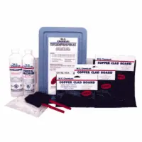
Circuit Specialists carries a number of low-priced photoresist developers manufactured by industry leader MG Chemicals. In addition to positive and negative developers for copper-clad boards, we stock ammonium persulfate, sodium persulfate, and ferric chloride copper etching solutions for your PCB projects.
Ferric Chloride, Photoresists, and the Art of Copper Etching
Printed circuit boards (PCBs) can be created in a variety of ways, with most PCB fabrication—even personal prototypes—occurring far from home in distant factories.
But there’s nothing quite as artful or satisfying as etching the copper-clad boards yourself. Plus, etching and fabricating PCBs from home is much faster (and cheaper!) than using a PCB fabrication service.
The very first working PCB was made by Austrian engineer Paul Eisler, who replaced radio tube wiring with a circuit he etched into copper foil on a non-conductive glass base. Today, we don’t free-hand etch connections into copper boards, but instead use a combination of photosensitive chemicals and etching solutions to fabricate PCBs.
This new and improved process, called photoengraving, is still used today and can be done from home! The following information provides a brief overview of this process, as well as the chemicals and supplies involved.
Etching Solutions & Photochemicals
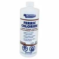
Ferric Chloride
Ferric Chloride is an inorganic compound with highly acidic and corrosive properties. In the electronics industry, ferric chloride is commonly used as a copper etching solution for PCB fabrication.
As an acid etching solution, ferric chloride can also be used in jewelry-making, metalsmithing, and many other metal etching applications.
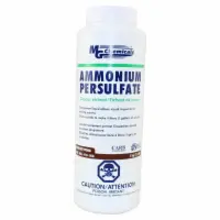
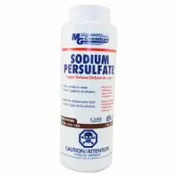
Ammonium Persulfate
Like Ferric Chloride, Ammonium Persulfate (APS) is a copper etching solution, although it’s less commonly used than Ferric Chloride.
Ammonium Persulfate is usually more expensive and slower-acting than Ferric Chloride is, but has the advantage of being much cleaner and easier to work with because it’s transparent and non-staining.
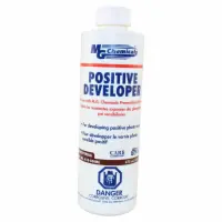
Photoresist
A photoresist is a light-sensitive material used during the PCB photoengraving process to form a protective mask or coating over the copper board. This photoresist mask is what protects parts of the board from the acid etching solution.
During the photoengraving process, a patterned mask (in this case, the circuit you plan to etch) is placed over the copper board. Then, the board is placed in either a negative or positive photoresist developer.
If using a positive photoresist developer, the developer then dissolves parts of the surface that were exposed to light and leaves behind a protective coating where the patterned mask was blocking light.
A negative photoresist developer will do the opposite, dissolving regions that were masked from light and coating areas exposed to light. Most PCB fabrication methods only use positive photoresists.
Once developed, the PCB is ready for the etching solution, which will remove all copper from the board except for the protected, coated sections created by the photoresist.
What is Photo Engraving?
Photoengraving*, sometimes called photo etching or photo chemical etching, is the process of using a light-sensitive chemical (photoresist) and an acidic etching solution (like Ferric Chloride) to fabricate a printed circuit board from scratch.
Instead of etching copper boards by hand, chemical etching allows people to essentially stamp their design onto the copper board and then bathe the board in a solution that dissolves most of the copper until only your design remains. The photoresist is what coats your design so that it can withstand the acidic metal etching process.
The process can be summed up in the following steps, although the process may look slightly different depending on the chemicals or techniques you’re using. We’ll only discuss positive photoresist developers since this is the most common developer used for photoengraving PCBs.
- A design or mask is placed over the copper board, effectively blocking light wherever the design is.
- The copper board is placed in a bath of positive photoresist developer, which creates a protective mask or coating over parts of the surface that are NOT exposed to light.
- After removing the board from the photoresist developer, the board is then added to a PCB etching solution, which will remove any copper or material that is not protected by the photoresist mask created by the developer.
- The PCB, now free of unnecessary copper because of the PCB etchant, is washed under running water.
- The photoresist mask, which protected your design during the etching process, is cleaned off via acetone and water.
*Note: Photoengraving is a process used in a variety of industries. For our purposes, we’re only covering this process as it applies to printed circuit boards.
Important Safety Considerations
As you should with any chemical, be mindful of the safety hazards associated with etching solutions and photoresist developers.
By nature, Ferric Chloride is a corrosive chemical that can be extremely harmful or even fatal if consumed or inhaled, causing tightness in the chest and breathing difficulties. These etching solutions can also severely irritate or burn skin and eyes upon contact. Misusing Ferric Chloride in the long term can even cause eye discoloration.
Positive photoresist developers have similar safety concerns, causing irritation to eyes, nose, and respiratory tracts upon exposure, including inhalation. The vapor and liquid is combustible, and Ferric Chloride can be a fire hazard as well.
To protect yourself, always work in a well-ventilated area and wear protective clothing, including gloves that are designed to work with corrosive chemicals. Read through and follow the safety recommendations included on the manual or bottle with your purchase.